
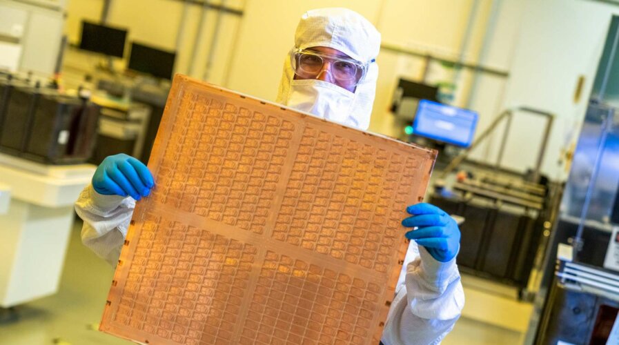
An Intel engineer holds a take a look at glass core substrate panel at Intel’s Meeting and Take a look at Expertise Improvement factories in Chandler, Arizona, in July 2023. Intel’s superior packaging applied sciences come to life on the firm’s Meeting and Take a look at Expertise Improvement factories. (Credit score: Intel Company)
- Intel introduced a major breakthrough in substrate supplies on superior packaging—and it’s all about glass substrate.
- Intel is anticipated to ship full glass substrate options to the market within the second half of this decade.
- It’s calculated that can permit the {industry} to proceed advancing Moore’s Legislation past 2030.
The advantages of Moore’s legislation are reaching their limits, which suggests chip efficiency advances are more and more counting on the again finish of manufacturingtogether with packaging. One answer has emerged to bridge the hole in technological development and meet the semiconductor market’s wants: superior semiconductor packaging expertise. For Intel, the reply for the subsequent era of semiconductors lies in glass substrates.
“By the tip of the last decade, the semiconductor {industry} will seemingly attain its limits on having the ability to scale transistors on a silicon package deal utilizing natural supplies, which use extra energy and embrace limitations like shrinkage and warping,” Intel stated when asserting its breakthrough innovation for its next-generation of superior packaging.
Emphasizing that scaling stays essential to the progress and evolution of the semiconductor {industry}, Intel introduced that it has begun a years-long transition to new expertise that rests processors on a mattress of glass as a substitute of at the moment’s epoxy-like natural resin. The brand new glass basis, referred to as substrate, provides the velocity, energy, and actual property needed for the chip {industry}’s shift to new expertise, packaging a number of “chiplets” right into a single bigger processor.
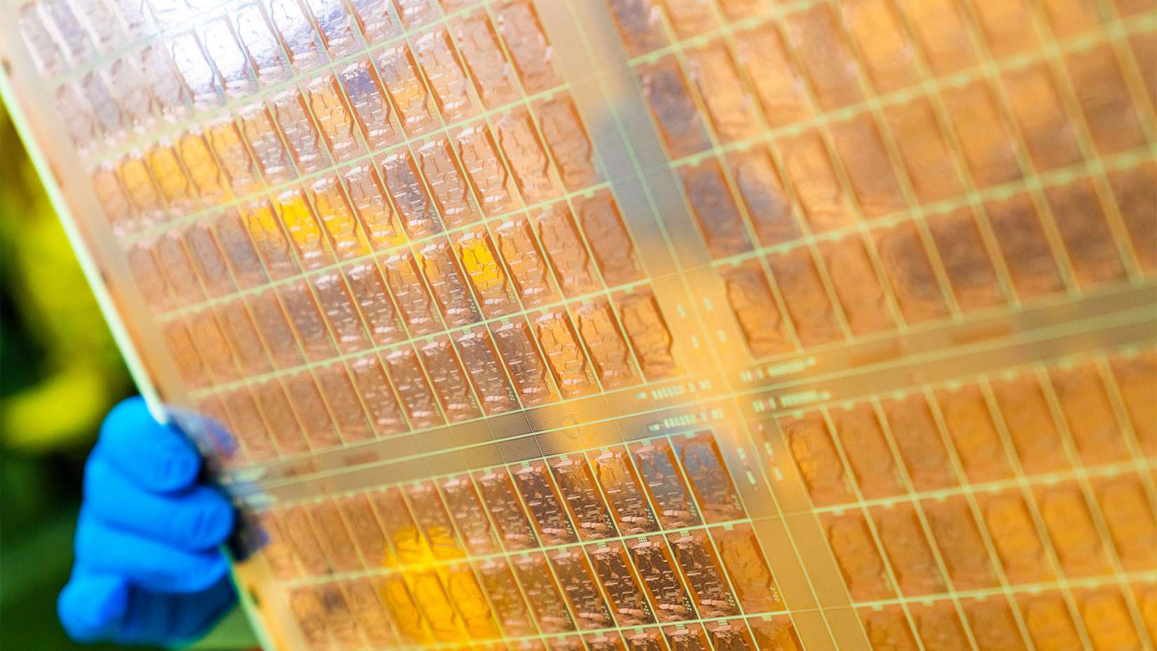
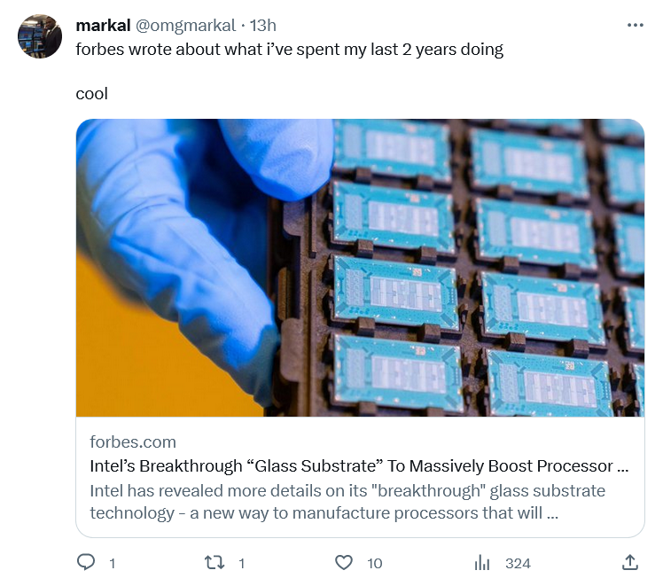
Intel delivers industry-leading packaging that permits efficiency, price and scaling advantages for Intel and Intel Foundry Providers clients. (Picture credit score: Intel)
What’s superior packaging?
Superior packaging helps meet the demand for semiconductors that run rising functions that at the moment are mainstream—particularly synthetic intelligence (AI). These functions require high-performance, low-power chips that quickly course of large quantities of information.
Regardless of the prediction by Intel co-founder Gordon Moore, who in 1965 posited that the variety of transistors on a microchip would double each couple of years, node development is now reaching its limits. Because of this, technical advances on the front-end of chip manufacturing are slowing, and the economically viable most measurement of a die, and thus its efficiency, have gotten extra restricted.
A photograph exhibits the ball grid array facet of an intel assembled glass substrate take a look at chip at intel’s Meeting and Take a look at Expertise Improvement factories in Chandier, Arizona, in July 2023. Intel’s superior packaging applied sciences come to life on the firm’s Meeting and Take a look at Expertise Improvement factories. (Credit score: Intel Company)
New approaches in back-end expertise that mix a number of chips provide a promising answer. Superior packaging strategies over the previous twenty years embrace 2.5-D, 3-D, fan-out, and system-on-a-chip (SoC) packaging—promising to fill the void by supplementing the wire-bonding and flip-chip applied sciences of the earlier half-century.
“As a result of superior packaging provides a higher-value alternative than conventional back-end packaging, main gamers and quick followers (organizations that imitate rivals’ improvements) are growing and commercializing numerous types of the expertise to win premium clients,” McKinsey said in its report in Might this yr.
What does Intel keep in mind?
Intel has relied on the chipset strategy to compete with superior processor manufacturing talents. For context, the A17 Professional processor in Apple’s iPhone 15 Professional has 19 billion transistorswhereas Intel’s Ponte Vecchio supercomputing processor has greater than 100 billion. Intel expects that by the tip of the last decade, processors might be made up of a trillion transistors as a result of glass substrates’ superior packaging.
Contemplating that we’re in an period of exploding demand for brand spanking new processing energy, Intel determined to flex its packaging prowess by unveiling the {industry}’s first glass substrates for next-generation superior packaging, deliberate for the latter a part of this decade. “This breakthrough achievement will allow the continued scaling of transistors in a package deal and advance Moore’s Legislation to ship data-centric functions,” Intel stated.
Babak Sabi, Intel senior VP and basic supervisor of meeting and take a look at improvement stated that reaching an industry-leading glass substrate for superior packaging had taken Intel a decade of analysis. “We sit up for delivering these cutting-edge applied sciences that can profit our key gamers and foundry clients for many years.”
How would glass substrate make a distinction for future chips?
In comparison with at the moment’s natural substrates, Intel stated glass provides distinctive properties equivalent to ultra-low flatness and higher thermal and mechanical stability, leading to a lot increased interconnect density in a substrate. These advantages permit chip architects to create high-density, high-performance chip packages for data-intensive workloads equivalent to AI.
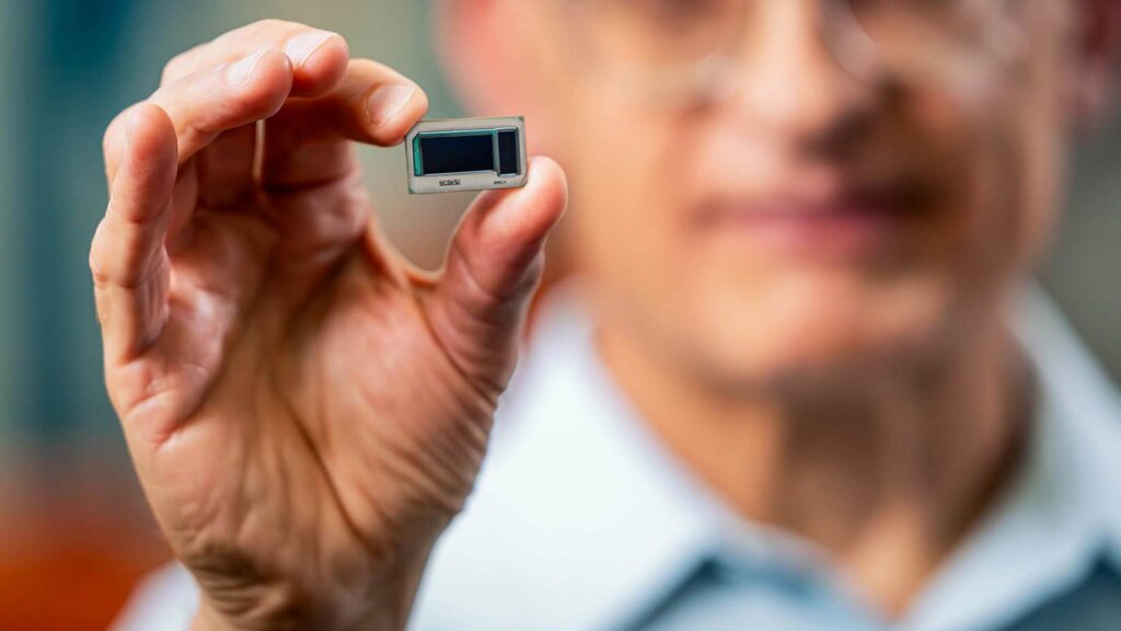
Hamid Azimi, company vice chairman and director of substrate expertise improvement at Intel Company, holds an Intel assembled glass substrate take a look at chip at Intel’s Meeting and Take a look at Expertise Improvement factories in Chandler, Arizona, in July 2023 (Credit score: Intel Company)
“Glass substrates can tolerate increased temperatures, provide 50% much less sample distortion, have ultra-low flatness for improved depth of focus for lithographyand have the dimensional stability wanted for very tight layer-to-layer interconnect overlay,” Intel stated, including {that a} 10x improve in interconnect density is feasible on glass substrates.
Intel added that improved mechanical properties of glass allow ultra-large form-factor packages with very excessive meeting yields. The US chip large is on observe to ship full glass substrate options to the market within the second half of this decade, permitting the {industry} to proceed advancing Moore’s Legislation past 2030.
Intel is banking on superior packaging to increase Moore’s Legislation.
“Glass substrates possess superior mechanical, bodily and optical properties that permit for extra transistors to be related in a package deal, offering higher scaling and enabling meeting of bigger chiplet complexes (referred to as “system-in-package”) in comparison with the natural substrates in use at the moment,” Intel added.
Briefly, chip architects can pack extra tiles – additionally referred to as chiplets – in a smaller footprint on one package deal whereas reaching efficiency and density good points with better flexibility and decrease total price and energy utilization.
“Because the demand for extra highly effective computing will increase and the semiconductor {industry} strikes into the heterogeneous period that makes use of a number of ‘chiplets’ in a package deal, enhancements in signaling velocity, energy supply, design guidelines, and stability of package deal substrates might be important,” Intel famous.
Which {industry} will profit first and most?
Intel believes that tumbler substrates will initially be launched into the market the place functions and workloads require bigger kind issue packages and better velocity capabilities. So, it is going to be extra substantial and helpful for information facilities, AI, and graphics.
“Constructing on the momentum of current PowerVia and RibbonFET breakthroughs, these industry-leading glass substrates for superior packaging show Intel’s ahead focus and imaginative and prescient for the subsequent period of computing past the Intel 18A course of node,” the chip large stated.
The corporate stated that since it’s on the trail to delivering one trillion transistors on a package deal by 2030, the continued innovation in superior packaging, together with glass substrates, will assist obtain this purpose.
Dashveenjit Kaur
| ![]() @DashveenjitK
@DashveenjitK
Dashveen writes for Tech Wire Asia and TechHQ, offering research-based commentary on the thrilling world of expertise in enterprise. Beforehand, she reported on the bottom of Malaysia’s fast-paced political enviornment and inventory market.