If you happen to look again at it now, particularly with the appearance of massively parallel computing on GPUs, perhaps the techies at Tera Computing after which Cray had the fitting thought with their “ThreadStorm” massively threaded processors and excessive bandwidth interconnects.
Provided that lots of the neural networks which are created by AI frameworks are themselves graphs – the sorts with vertices with knowledge and edges displaying the relationships between the information, not one thing generated in Excel – or output what quantities to a graph, perhaps, ultimately, what we’d like is a extremely good graph processor. Or, perhaps thousands and thousands of them.
Gasp! Who speaks such heresy in a world the place the Nvidia GPU and its wannabes are the common unguent to resolve – salvecertainly? – our trendy computing issues? Effectively, we do. Whereas GPUs excel at dense matrix excessive precision floating level math that dominates HPC simulation and modeling, lots of the information that underpins AI frameworks is sparse and decrease precision besides. And given this, perhaps there are higher methods to do that.
The US Protection Superior Analysis Tasks Company, the analysis and improvement arm of the Division of Protection, explores simply such leading edge questions, and has been wanting into making a massively parallel graph processor and interconnect since establishing the Hierarchical Determine Confirm Exploit (HIVE) mission again in 2017. Intel was chosen to make the HIVE processor and Lincoln Laboratory at MIT and Amazon Net Companies have been chosen to create and host a trillion-edge graph dataset for a system based mostly on such processors to chew on.
At Sizzling Chips 2023 this week, Intel was displaying off the processor it created for the HIVE mission, which was initially codenamed “Puma” in relation to the Programmable Built-in Unified Reminiscence Structure (PIUMA) that underpins it. In August 2019, Intel gave an replace on the PIUMA chip at DARPA’s ERI Summit, and on the IEEE’s Excessive Efficiency Excessive Computing 2020 occasion in September 2020, Intel researchers Balasubramanian Seshasayee, Joshua Fryman, and Ibrahim Hur gave a presentation referred to as Hash Desk Scalability on Intel PIUMAwhich is behind an IEEE paywall however which gave an summary of the processor, and a paper referred to as PIUMA: Programmable Built-in Unified Reminiscence Structurewhich isn’t behind a paywall. These have been imprecise in regards to the structure of the PIUMA system. However this week, Jason Howard, a principal engineer at Intel, gave an replace on the PIUMA processor and system, together with a photonics interconnect that Intel has created at the side of Ayar Labs to lash an infinite variety of processors collectively.
Within the IEEE paper, the PIUMA researchers made no bones about the truth that they have been completely impressed by the Cray XMT line. The XMT line from a decade in the past culminated with a large shared reminiscence thread monster that was good for graph evaluation, which had as much as 8,192 processors, every with 128 threads operating at 500 MHz, plugging into an AMD Rev F socket utilized by the Opteron 8000 sequence of X86 CPUs all lashed along with a customized “SeaStar2+” torus interconnect that delivered 1.05 million threads and 512 TB of shared important reminiscence for a graph to stretch its legs upon. So far as Linux was involved, this appeared like a single CPU.
What’s outdated is new once more with the PIUMA mission, and this time the processor is extra modest however the interconnect is significantly better. And presumably the worth/efficiency is as properly, and for the love of all that’s holy in heaven, maybe Intel will commercialize this PIUMA system and actually shake issues up.
Taking Smaller Bytes Of Reminiscence
When Intel began out designing the PIUMA chip, based on Howard, the researchers engaged on the HIVE mission realized that graph jobs weren’t simply massively parallel, however embarrassingly parallel, which implies there have been most likely some methods to use that parallelism to drive up the efficiency of graph analytics. When operating on normal X86 processors, graph databases had very unhealthy cache line utilization, with solely 8 bytes or much less of a 72 byte cache line getting used over 80 % of the time a graph database was operating. Having tons and many branches within the instruction stream put stress on the CPU pipelines and the reminiscence subsystem additionally had lots of strain on it from lengthy chains of dependent hundreds, which thrashed the caches on the CPUs.
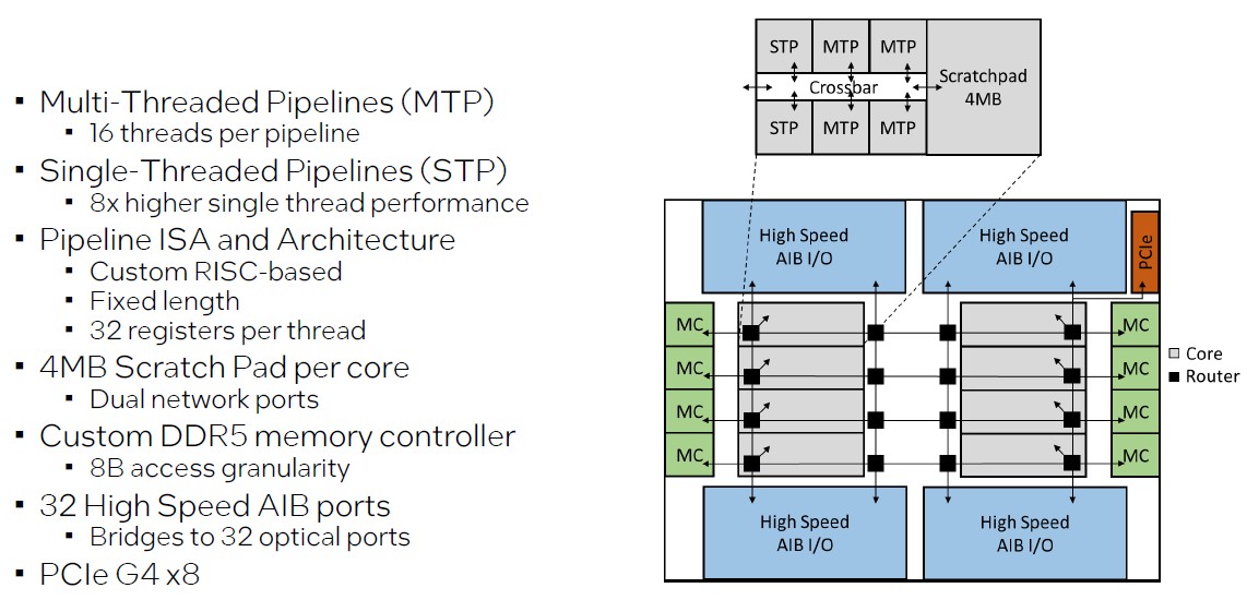

The PIUMA chip has some big-little concepts embedded with it, and has 4 pipelines which have 16 threads per pipeline (referred to as MTPs) and two pipelines which have a single thread every (referred to as STPs) that ship 8X the efficiency of one of many threads inside the MTPs. The cores are based mostly on a customized RISC instruction set, which Howard didn’t determine and neither have his analysis friends at Intel or Microsoft, which has additionally had a hand within the PIUMA effort.
“All of the pipelines use a customized ISA, it’s RISC-like, it’s a hard and fast size,” defined Howard in his Sizzling Chips presentation. “And every of the pipeline has 32 bodily registers accessible to it. We did this in order that you might simply migrate compute threads between any of the pipelines. So perhaps I begin out executing on one of many multithreaded pipelines and if I see that it’s taking too lengthy, or perhaps it’s the final thread accessible, I can migrate that shortly over to my single thread pipeline to get higher efficiency.”
The STP and MTP models are related by a crossbar and have a mixed 192 KB of L1 instruction and L1 knowledge cache, they usually hyperlink to a shared 4 MB scratchpad SRAM reminiscence that’s easier than an L2 cache.
Every PIUMA chip has energetic eight cores, and every core has its personal customized DDR5 reminiscence controller that has 8 byte entry granularity as a substitute of 72 byte granularity like regular DDR5 reminiscence controllers do. Every socket has 32 GB of that customized DDR5-4400 reminiscence.
Every core has a pair of routers that hyperlink the cores in a 2D mesh to one another, to the eight reminiscence controllers, and to 4 excessive pace Superior Interface Bus (AIB) ports. AIB is a royalty-free PHY for interconnecting chiplets that Intel introduced again in 2018. There are 32 optical I/O ports, eight per AIB, that come off the die enhances of Ayar Labs, which ship 32 GB/sec of bandwidth in every route.
Here’s a drilldown on the on-chip routers that implement the 2D mesh on the PIUMA bundle:
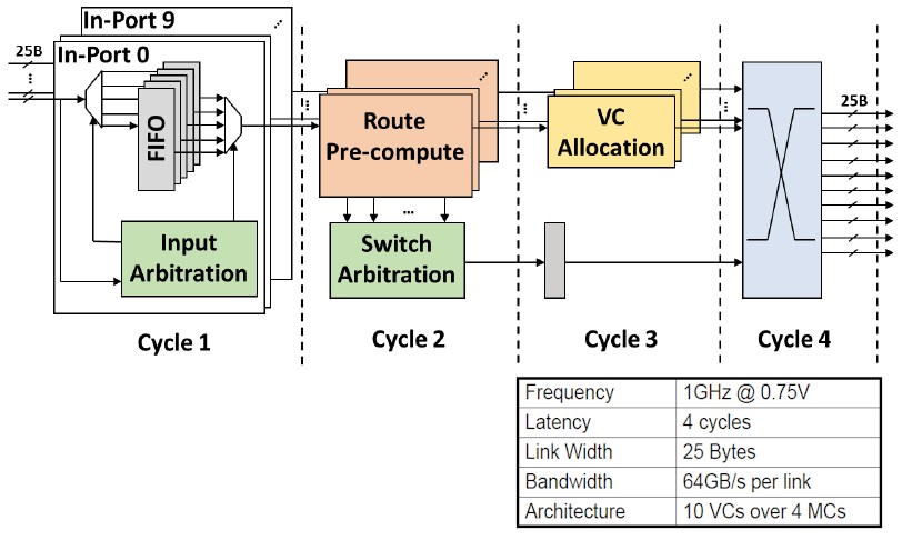

This can be a ten port, cut-through router The 2D mesh runs at 1 GHz and it takes 4 cycles to traverse the router. It has ten digital channels and 4 completely different message lessons, which Howard says avoids any deadlocks on the mesh and which yield 64 GB/sec for each hyperlink inside the router.
The router and core packaging on the PIUMA chip is a little more advanced than you may count on. Have a look:
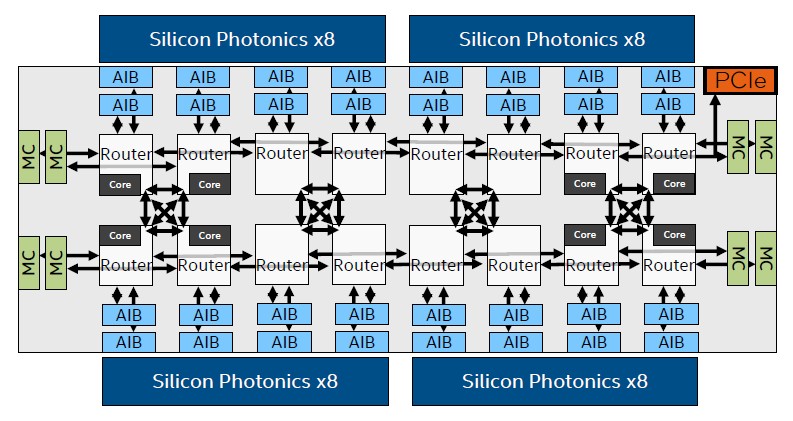

It’s extra like there are sixteen core/router models on the die, and solely eight of them have the cores activated as a result of the on-die mesh wants twice as many routers to feed into the AIBs, which in flip feed into the Ayar Labs silicon photonics. The silicon photonics hyperlinks are solely used as a bodily layer, and they’re used particularly to increase the on-die community between a number of sockets.
And once we say a number of, we imply a freaking big quantity. Like this:
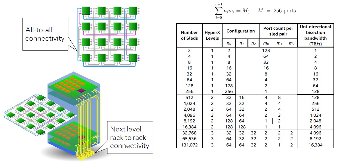

A sled of sixteen these PIUMA chips utilizing the silicon photonics hyperlinks could be linked collectively in a 4×4 grid in an all-to-all configuration. Every PIUMA chip burns round 75 watts at nominal voltage and workloads, which implies a it burns round 1,200 watts. Greater than a Xeon SP socket, however no more than three of them.
Constructing The Excellent Graph Processing Beast
The PIUMA chip has 1 TB/sec of optical interconnect popping out of it, and apart from the on-sled hyperlinks, a few of them can be utilized to attach as much as 131,072 sleds collectively to make a large shared reminiscence graph processing supercomputer. The routers are the community, and every thing is related by a HyperX topology outdoors of the instantly connected-all-to-all topology inside a rack, which has sixteen sleds.
Let’s stroll by means of this. A single sled with sixteen sockets has 128 cores with 8,448 threads and 512 GB of reminiscence. The primary stage of the HyperX community has 256 sleds, 32,768 cores, 270,336 threads, and 1 TB of reminiscence. Step as much as stage two of the HyperX community, and you’ll construct out a PIUMA cluster with 16,384 sleds, 2.1 million cores, 17.3 million threads, and 64 TB of shared reminiscence. And eventually, up at stage three of the HyperX community, you possibly can broaden out to 131,072 sleds, 16.8 million cores, 138.4 million threads, and 512 PB of shared reminiscence.
Admit it. You wish to see what one among these beasts might do. The US Nationwide Safety Company and the Division of Protection in america and their friends world wide, who’ve funded lots of the AI analysis prior to now fifteen years, little doubt have an interest, too.
As you chew on that scale for a minute, let’s go over a couple of extra issues. First, the latency of that optical community:
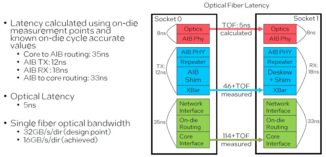

The PIUMA nodes are linked along with single-mode optical fiber, and it’s attention-grabbing that the achieved bandwidth of the PIUMA community design, at 16 GB/sec per route, was solely have the of the theoretical design level. However even nonetheless, it is a big bandwidth beast, with a theoretical 16 PB/sec of uni-directional bisection bandwidth throughout the complete HyperX community.
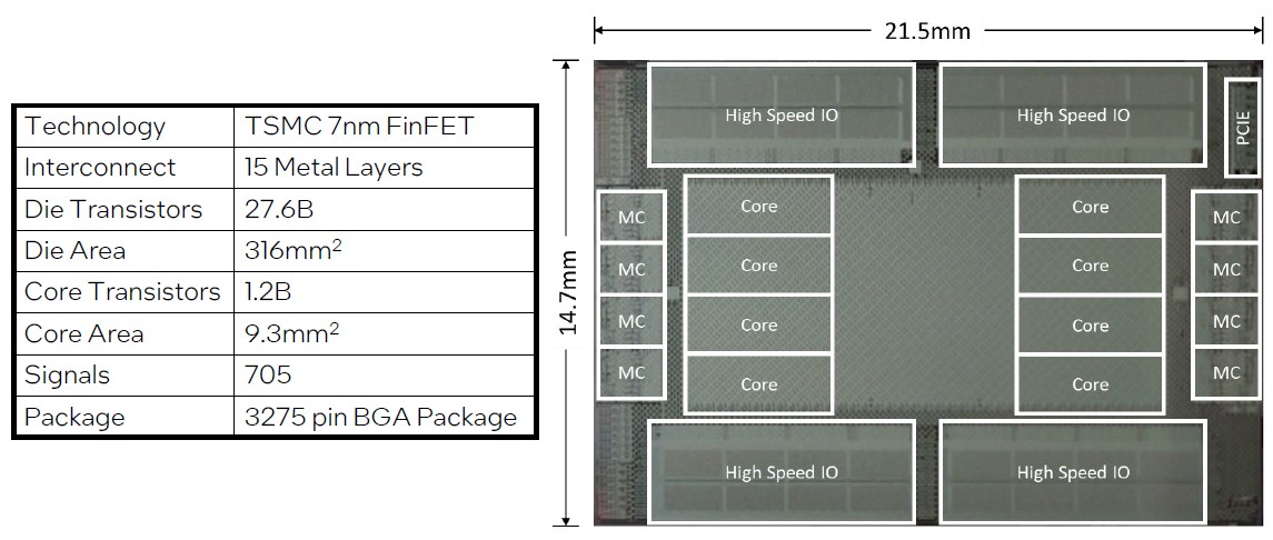

The PIUMA chip is carried out in 7 nanometer FinFET processes from Taiwan Semiconductor Manufacturing Co, and it has 27.6 billion transistors on it with 1.2 billion of them being devoted to the comparatively small cores. The AIB circuits take up lots of the transistor depend, apparently.
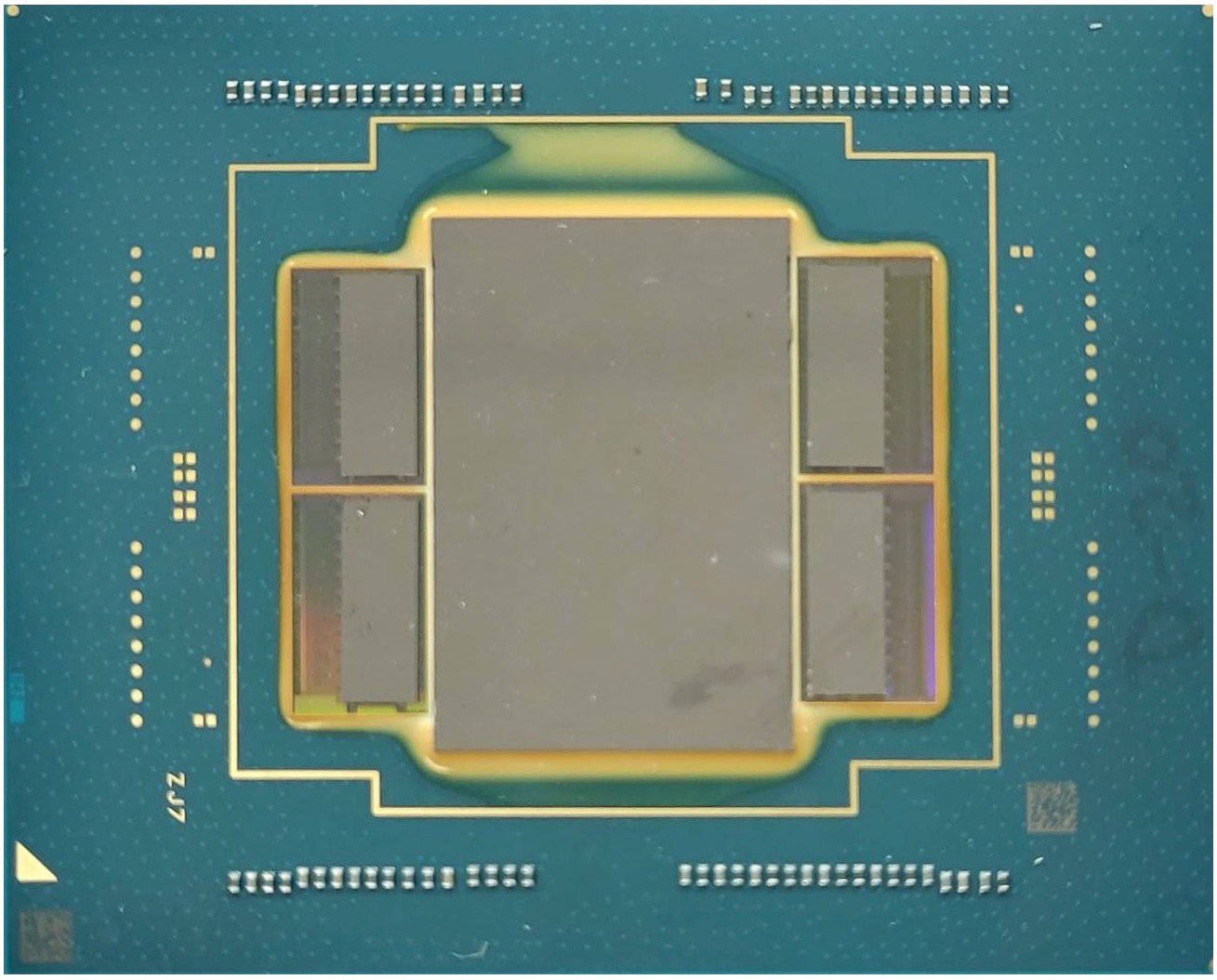
Here’s what the PIUMA chip bundle seems to be like:

And here’s what the bundle and check boards appear to be:
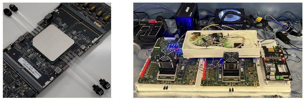

To this point, Intel has constructed two boards with a single PIUMA chip every and interlinked them to runs its checks and to show to DARPA that it really works.
The query now could be, what’s going to such a machine value at scale? Effectively, at $750 per node, which ain’t a lot in any respect, it’s $3.1 million for a system prolonged to HyperX stage one with 4,096 PIUMA chips, near $200 million for one with 262,144 chips at HyperX stage two, and $1.57 billion for one with 2.1 million chips stretched to HyperX stage three.
Because the generative AI explosion exhibits, there are a number of dozen corporations after which one other a number of dozen authorities businesses on the earth that received’t even blink at $1 billion for a system anymore. The quantity didn’t even increase my pulse once I wrote it after which learn it.
That’s simply the time we dwell in now.