
Stable-state drives (SSDs) have considerably advanced information storage, transferring away from the mechanical design of Arduous Disk Drives (HDDs) in the direction of a extra environment friendly, semiconductor-based method. SSDs use flash reminiscence, which offers quicker information entry, elevated sturdiness, and larger power effectivity. This text goals to demystify the complicated expertise behind SSDs, specializing in their elements and the way they handle information storage and retrieval.
Construction of an SSD and its elements
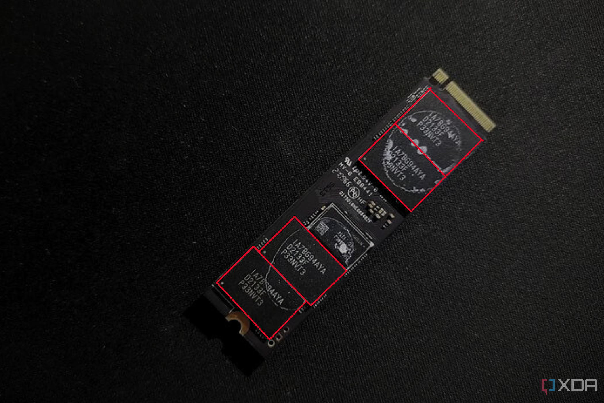 NAND Flash
On the coronary heart of an SSD lies its built-in circuit, a posh meeting of digital circuits intricately embedded inside a silicon semiconductor cell. This integration is vital to the SSD’s skill to retailer huge information in a compact kind issue.
SSDs depend on flash reminiscence for information storage, characterised by its non-volatile nature. Because of this information is retained even when the SSD is just not powered. The construction of this flash reminiscence in SSDs relies on NAND expertise, the place information is organized right into a grid of blocks, every comprising an array of pages or sectors. These are the smallest models for information storage and entry inside the SSD. The environment friendly group and accessibility of those blocks and pages are what allow SSDs to supply pace and efficiency, considerably outstripping the capabilities of conventional onerous disk drives.
The basic mechanism for information storage in SSDs is offered by floating gate transistors (FGTs) inside the NAND flash reminiscence. These transistors have the distinctive skill to carry {an electrical} cost, which is used to symbolize binary information. The microscopic transistors and capacitors in SSDs might be charged to symbolize “1” or discharged to symbolize “0” by making use of completely different voltages, thereby storing or releasing a tiny quantity of electrical cost in a managed method. This means of manipulating electrical prices at a microscopic degree permits SSDs to realize exceptionally quick information entry speeds, far surpassing the efficiency of HDDs.
SSD controller

The SSD controller, a classy microprocessor that acts like a CPU, is central to the drive’s performance and efficiency. It manages a collection of complicated algorithms, every designed to optimize information dealing with and storage longevity. One key algorithm is put on leveling, which intelligently distributes information written throughout the NAND flash reminiscence. This technique mitigates the uneven put on of reminiscence cells so that every cell has the identical approximate longevity. By making certain that no single cell is overused, put on leveling considerably extends the SSD’s total lifespan. Error Correction Code (ECC) is one other essential algorithm. As information integrity must be ensured within the steady coding and decoding, ECC algorithms work relentlessly to detect and proper bits of knowledge which will have been altered or corrupted throughout storage or transmission.
This course of includes producing further information bits throughout writing, that are used for comparability and error correction throughout studying. The sophistication of ECC algorithms instantly influences the reliability and accuracy of knowledge retrieval in SSDs. Moreover, the controller executes unhealthy block mapping, figuring out and isolating broken or worn-out cells (unhealthy blocks). It then remaps information storage to wholesome cells, making certain information integrity and constant efficiency. This proactive administration prevents information loss and maintains the drive’s effectivity.
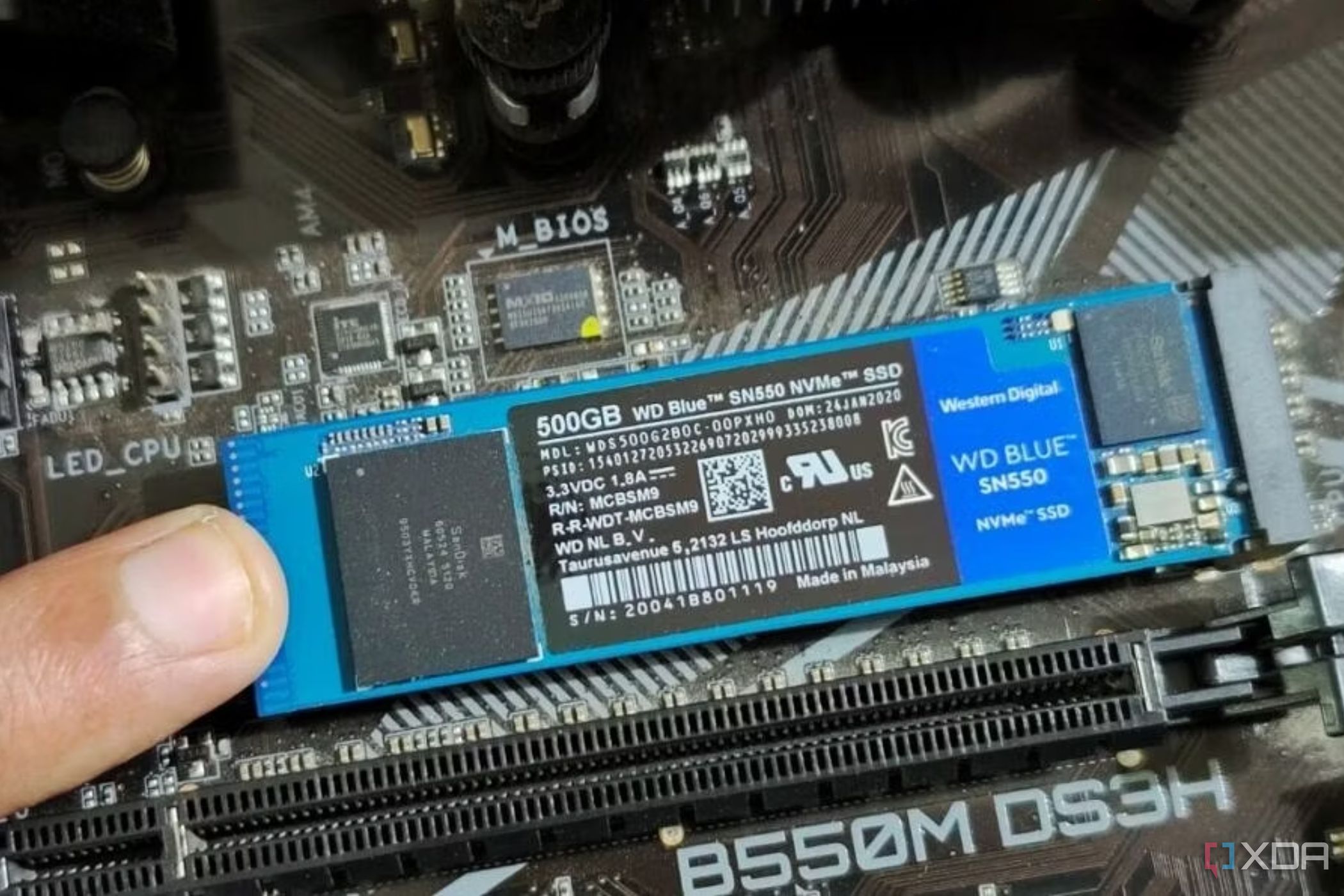
DRAM Cache
Many SSDs embody a DRAM cache, which serves as a fast-access reminiscence pool for storing short-term information and mapping tables (the listing to the situation of all the information). This considerably hurries up information retrieval processes, lowering the time it takes for the SSD to find and entry information. The DRAM cache is a key element in enhancing the general responsiveness and effectivity of an SSD.
How does information storage work in SSDs?
Writing information
Writing information to an SSD is a exact and sophisticated course of. It begins with information encoding, which converts info right into a format appropriate for storage utilizing the Error-Correcting Code (ECC). Information is then written in ‘pages,’ which is the smallest unit of knowledge for writing. Nevertheless, erasing information requires clearing total ‘blocks,’ that are teams of pages. This attribute necessitates the Program/Erase cycle, the place a full block is erased and rewritten, even for small information adjustments. Put on leveling (dealt with by the controller) comes into play right here, because the controller spreads out these cycles throughout the reminiscence cells to forestall any single cell from being overused and worn out prematurely.
Studying information
Studying information from an SSD includes the controller finding the proper block and web page. It then reads the saved cost from the reminiscence cells, decoding this as binary information. Throughout this course of, ECC algorithms detect and proper errors, making certain the accuracy and integrity of the retrieved information.
NAND flash varieties and their impacts
1. SLC (Single-Degree Cell) NAND:
SLC NAND shops one bit per cell, offering the very best pace and endurance amongst NAND varieties. This makes it perfect for high-performance purposes however comes at a better value attributable to its decrease storage density and extra complicated manufacturing course of.
2. MLC (Multi-Degree Cell) NAND:
MLC NAND shops two bits per cell, placing a steadiness between value and efficiency. It’s cheaper than SLC attributable to larger information density however has reasonably decrease pace and endurance. MLC is usually utilized in consumer-grade SSDs and enterprise purposes the place a steadiness of efficiency and price is critical. The time period MLC can apply to any cell that shops multiple bit per cell, nevertheless it’s extra generally used for two-bit cells.
3. TLC (Triple-Degree Cell) NAND:
TLC NAND, storing three bits per cell, gives even larger value effectivity by rising the storage density. Nevertheless, this comes on the expense of decreased pace and lifespan in comparison with MLC. TLC NAND is commonly utilized in budget-friendly SSDs the place giant storage capability is prioritized over top-tier efficiency.
4. QLC (Quad-Degree Cell) NAND:
QLC NAND, with 4 bits saved per cell, offers the very best density for storage, translating to the biggest capability on the lowest value. Nevertheless, this benefit is offset by the bottom endurance and slower efficiency relative to the opposite varieties. QLC is appropriate for purposes the place storage capability is extra essential than pace or longevity, like in some shopper storage gadgets.
Issues with SSDs

Write amplification is a phenomenon in SSDs the place the precise quantity of knowledge written exceeds the supposed information. This happens in the course of the Program/Erase cycle and might adversely have an effect on the SSD’s lifespan. Moreover, SSDs make use of a course of known as rubbish assortment, which includes rearranging and consolidating information for environment friendly reminiscence block utilization. Whereas important for sustaining optimum storage effectivity, rubbish assortment can briefly hinder SSD efficiency, notably throughout heavy data-writing operations.
Over time, the repeated use of NAND cells in SSDs results in information degradation, impacting efficiency and longevity. To counteract this, strategies resembling over-provisioning are used, the place further storage capability is reserved to exchange worn-out cells. Moreover, the TRIM command performs an important position by enabling the working system to inform the SSD of which information blocks are now not in use, permitting for extra environment friendly information administration and serving to to protect the well being and effectivity of the SSD over its lifespan.