
Intel has frequently advanced its processor socket design, introducing a sequence of upgrades since Socket 1151 in 2015. The transition moved from Socket 1200 with the tenth-generation Core i (Comet Lake) in 2020 to the Base 1700 for the twelfth-generation (Alder Lake). The newest launch, the Raptor Lake Refresh, belongs to the 14th Intel Core technology. Meteor Lake’s launch, initially anticipated for the current 12 months, was postponed because of the introduction of a chiplet structure, primarily confined to the cell sector labeled “Core Extremely.”
Set for a 2024 launch, Arrow Lake-S represents Intel’s forthcoming Core technology for desktops. Accompanying this fifteenth technology, a brand new socket, LGA1851, is anticipated, rising the pin depend by 151 from its antecedent. Benchlife.org supplies a graphic depicting this format.
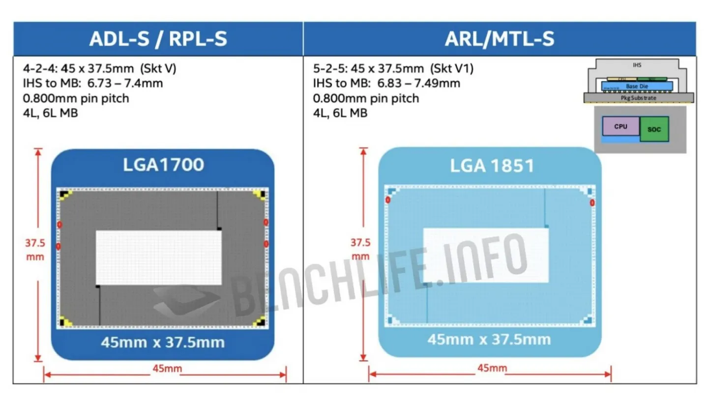
The brand new socket, LGA1851, maintains the LGA1700’s dimensions, at 45×37.5 millimeters. The pin pitch stays constant, although there’s an enhancement in touch density. Changes within the warmth spreader’s peak, from 6.73 to 7.4 millimeters, will facilitate stacked chiplets. Current CPU coolers appropriate with LGA1700 are anticipated to suit LGA1851, with mounting distances retained. Notably, the utmost contact strain for LGA1851 will expertise an 89% increment from LGA1700. Intel is projected to again the LGA1851 socket with subsequent CPUs till 2026, doubtlessly supporting processors like Lunar Lake and Panther Lake. The 2026-slated Beast Lake/Nova Lake processors may also be congruent.
New insights about Arrow Lake-compatible processors recommend a big enhance within the L2 cache for the P cores. From Skylake’s 256 Kbytes L2 cache per core, subsequent generations witnessed regular increments. Rocket Lake had 512 KB, Alder Lake had 1.25 MB, and Raptor Lake carries 2 MB per core. Remarkably, Arrow Lake is projected to outfit P cores with an ample 3 MB L2 cache, enhancing efficiency by facilitating swifter information set entry. This efficiency leap can partly be attributed to the transition to the environment friendly 3nm manufacturing course of.
Intel’s roadmap suggests LGA1851 will embrace DDR5 RAM, reaching speeds as excessive as 7500 megahertz. This surpasses LGA1700 and Raptor Lake Refresh, which tops out at 5600 megahertz, indicating a phasing out of DDR4 RAM. Modifications are forthcoming for PCIe lanes. The intention is to combine a further 4 connection traces, harnessing all 20 PCIe 5.0 lanes. Current Intel CPUs, whereas having 20 lanes, can solely make use of 16 concurrently. This transformation permits simultaneous, optimum connections for each a graphics card and an M.2 SSD. An M.2 SSD’s connection through the CPU presently reduces the graphics card interface to eight lanes. There’s additionally an anticipated rise in PCIe 4.0 lanes, facilitating the linkage of one other 4.0 SSD with 4 lanes. Regardless of not equalling AMD’s AM5 socket, this can be a appreciable development, allowing a connection of not less than two PCIe 5.0 SSDs with 4 lanes every.