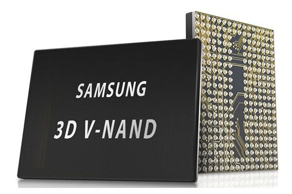
ComputerBase.de has reported that Samsung plans to disclose their new 280-layer QLC NAND chips on the Strong-State Circuits Convention (ISSCC). These NAND chips boast knowledge densities of 28.5 Gb per sq. millimetre. For context, that’s 50% greater than the info density of Micron’s current-generation 232-layer QLC applied sciences.

With this new NAND, Samsung hopes to energy new QLC-powered SSDs which can be extra knowledge dense and performant than their predecessors. With their new 1 Tb 280-layer QLC NAND chips, Samsung have claimed to supply 3.2 GB/s I/O charges. That is a lot sooner than Samsung’s current QLC NAND chips, suggesting that the corporate’s new QLC flash will allow the creation of sooner, greater capability QLC-powered SSDs. Maybe 16TB M.2 SSDs could possibly be constructed utilizing this new NAND?
Larger storage speeds and elevated knowledge densities will enable Samsung’s new NAND chips to disrupt the SSD market. Larger knowledge densities lower the price/GB of NAND flash. In less complicated phrases, the extra Terabytes of NAND that Samsung can get out of a silicon wafer, the higher.
We anticipate to listen to much more about Samsung’s new NAND chips on the Strong-State Circuits Convention (ISSCC). Will Samsung’s new QLC NAND have the identical efficiency downsides as different QLC chips when hit with sustained writes? Will it depend on SLC caching to take care of excessive write speeds? Will this NAND be obtainable to SSD producers quickly? We’ll know extra quickly.

You’ll be able to be part of the dialogue on Samsung’s 280-layer V9 QLC NAND on the OC3D Boards.