
“Intel’s in a fantastic spot,” stated company vp and APJ normal supervisor Steve Lengthy, including that its “execution and innovation engine is alive and effectively.”
The plan to introduce 5 nodes inside 4 years is on observe, with the Intel 7 course of (beforehand referred to as 10nm Enhanced SuperFin) in excessive quantity manufacturing, Intel 4 (7nm) manufacturing ramping up because the anticipated launch of the Meteor Lake household approaches, Intel 3 (3nm class) prepared to enter manufacturing this yr, and Intel 20A (2mn class) and Intel 18A (1.8nm class) anticipated to be prepared for manufacturing within the first and second half of 2024 respectively.
One other a part of Intel’s plan is “democratising AI,” he stated.
loadposition stephen08
AI capabilities might be in-built throughout the corporate’s product strains, together with Arc, Core, Xeon, GPUs (presumably together with the awaited 100 billion transistor Ponte Vecchio GPU), and the Habana and Gaudi knowledge centre processors.
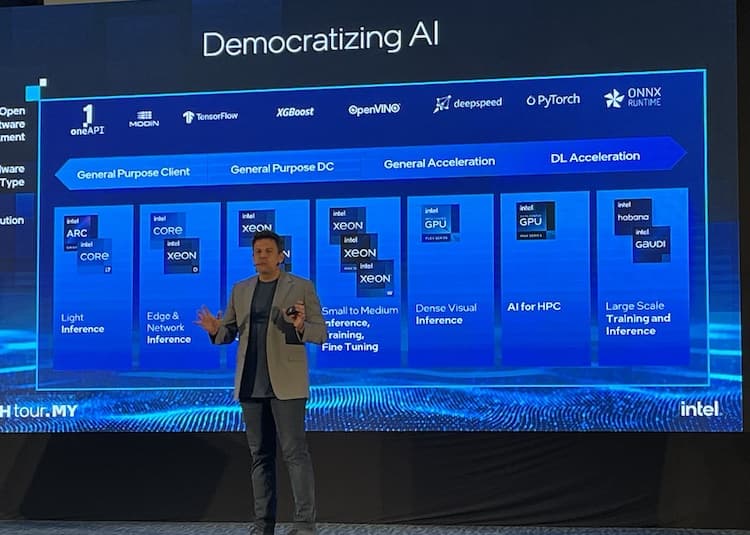
These “heterogeneous architectures” will permit Intel to supply the “proper merchandise for the correct resolution,” with the oneAPI toolkits simplifying software program growth throughout the totally different processors.
“We need to decrease the barrier to everybody,” stated Lengthy, and oneAPI meets clients’ need for open slightly than proprietary toolkits.
Intel normal supervisor of know-how options and APJ CTO Alexis Crowell stated the corporate has been following a method to democratise AI for seven or eight years. Simply as we now count on a laptop computer to incorporate a Wi-Fi interface, we are going to quickly be on the level the place new computer systems have instruction units assist the forms of operations wanted for AI.
However this “AI all over the place” alternative can’t be met with a “one measurement matches all” method: a 700W chip may be positive in a knowledge centre, however it’s no good for a laptop computer or different edge gadget. So to make it work, “you have to simplify the software program stack,” she stated, and “you have to get everybody within the ecosystem to rally round” – therefore oneAPI.
“Folks need to have the ability to select” between {hardware} distributors akin to Intel and Nvidia, she asserted. “We are able to completely problem in that house,” and in any case there may be room for multiple resolution.
Intel’s ecosystem method is an space the place “1+1=3,” she urged, as open and accessible platforms imply quicker advances. “We need to be one of the best know-how companion” offering the applying builders with the correct {hardware} and software program.
Crowell famous that the velocity of AI adoption varies between areas, and “what adjustments are the rules behind the use instances.” Intel desires to be a task mannequin for accountable AI, she stated.
The prospect of supporting AI in edge and shopper merchandise is “tremendous thrilling,” Intel shopper computing group vp Gokul V Subramaniam stated. “PCs are going to be central to bringing AI to scale” as a result of they’re used when persons are focussed on their work.
However “if you happen to do not begin with the enterprise downside, you possibly can’t get to the know-how,” stated Crowell. “In lots of instances you do not want one thing loopy costly” – as a substitute you could possibly do the job with capabilities already in your {hardware}, and that may grow to be more and more seemingly with forthcoming techniques.
Manufacturing
Intel’s angle in direction of openness may also be seen in its IDM 2.0 (built-in gadget manufacturing model 2.0) mannequin, which sees the corporate’s personal factories getting used for manufacturing at scale together with the expanded use of third-party foundries to offer further quantity in addition to the pliability that comes from having the ability to combine and match chiplets from a number of distributors. The latter functionality might be supported by the UCIe (Common Chiplet Interconnect Categorical) commonplace that can be supported by TSMC and Qualcomm, amongst others).
“That is the trail ahead,” he stated.
The third leg of IDM 2.0 sees Intel Foundry as a world-class enterprise open to clients and rivals. It’s already being utilized by Mediatek, Cisco, Amazon and Ericsson. Arm proposes to construct future low-power SoCs on Intel 18A, whereas Synopsys will use the Intel 3 and Intel 18A processes.
Intel vp and managing director of Intel Malaysia A.Okay. Chong defined that IDM 2.0 is a part of a method to make Intel the world’s largest foundry by the tip of the last decade.
The corporate will proceed constructing merchandise in its personal factories, however will use exterior capability strategically.
Turning to manufacturing in Malaysia, he recalled that it began with 100 staff manually assembling DRAM chips. In the present day, 15,000 folks work in 900,000 sq. toes (round 84,000 sq. metres), and additional growth is underway on the Penang and Kulim websites – the brand new four-storey superior packaging facility beneath development in Penang incorporates the piece of land the place the primary Malaysian manufacturing unit stood.
These developments will give the corporate some two million sq. toes (round 186,000 sq. metres) of producing house.
But it surely’s not simply manufacturing. The design and growth lab has designed merchandise together with SoCs, CPUs, chipsets and FPGAs. It’s concerned in product growth points akin to manufacturability and high quality, platform and system validation, and works with clients which might be integrating Intel merchandise into their very own.
“Intel Malaysia is sort of a little Intel,” Chong noticed, as most capabilities are carried out inside the nation. The primary exception is fabrication: the wafers that Intel Malaysia turns into completed merchandise come from the corporate’s foundries in locations akin to Israel.
Like different corporations, Intel Malaysia is addressing sustainability points. Chong stated it operates Intel’s largest photo voltaic farm outdoors the US, is 84% of the best way to attaining net-positive clear water, lower than 1% of its waste went to landfill in 2022, and it’s growing lower-carbon merchandise.
Subramaniam stated the corporate sees sustainability as an “finish to finish lifecycle alternative” that features manufacturing, working (eg, efficiency per watt, repairability and upgradability), and finish of life dealing with. That final level must be seen as together with “finish of first life” because it contains securely eradicating content material from a tool so it may be given or bought to another person for additional use earlier than lastly being taken out of fee and recycled to the extent potential.
As you may think, testing is a giant a part of semiconductor manufacturing.
Testing at Intel Malaysia begins earlier than designs are was actuality. New merchandise are emulated and examined with artificial instruments in addition to with actual purposes and benchmark packages working beneath goal working techniques together with Home windows and Ubuntu.
Related exams are carried out when the design has grow to be a prototype product. Automated processes load a BIOS and working system, together with an utility that may confirm the operation of the options being examined. At this stage, the product may be examined with industrial BIOSes and firmware, and AI is used to assist guarantee check protection, together with check suites designed to train multi-core and multi-module merchandise.
Earlier than a brand new product is launched, samples are examined to make sure the ability and efficiency are inside specs utilizing inner and exterior benchmarks. These exams are carried out together with real-world firmware, BIOS and drivers, however they use reference motherboards with further options permitting simple and intensely correct measurement in addition to the era of surprising situations akin to injecting a selected waveform into the ability strains. Once more, these exams are run at a variety of temperatures. One of many targets is to ascertain whether or not a design actually is correct for a selected section akin to skinny and lightweight notebooks. If not, the lab works with the product design group to deal with the difficulty, maybe by rebalancing energy and efficiency.
Put up-silicon practical validation begins with figuring out easy methods to confirm the operation of latest chips. The group wants to find out what to check and easy methods to check it. One of these testing includes a number of {hardware}, a number of cycles, and typically a number of time. Basically, an goal is to train as a lot of the gadget as potential within the time accessible, so the lab is ready as much as check a number of configurations concurrently. When points are detected, varied debugging instruments are used to offer suggestions to the product group.
The lab additionally works with clients to assist check and optimise merchandise beneath growth that use Intel processors. A part of the job is to develop testing strategies for brand spanking new applied sciences akin to DDR6 reminiscence. Prospects give you a variety of potential configurations round every Intel processor, so testing must be equally versatile with the intention to deal with potential thermal and energy points, in addition to checking the steadiness between efficiency and energy consumption.
Electrical validation is a part of the system validation course of. A part of that is sign integrity validation: does a selected interface (eg, PCIe Gen 5) work accurately throughout all configurations and working situations? A mix of software program automation and robotic dealing with is used to hurry testing, so a machine picks up the processor, checks its orientation, locations it within the socket, and positions a thermal tester on high of it. The suite of exams are run (with the outcomes being made accessible to distant customers, who can specify the exams to be run), after which the processor is eliminated so the subsequent one may be examined.
As soon as manufacturing has begun, wafers arrive from Intel fabs such because the one in Israel and are sawn into particular person chips. This course of includes mounting the wafer on a mylar sheet coated with an adhesive that’s robust sufficient to carry the wafer and its constituent chips through the sawing course of. It’s then uncovered to ultraviolet gentle, which weakens the adhesive sufficiently to permit the chips to be eliminated. Every chip is then examined for defects and sorted in keeping with its efficiency. Removing defective chips at this stage avoids losing assets throughout subsequent manufacturing phases.

The testing course of is extremely automated. Trays of newly-separated chips are grouped in packing containers, and these packing containers are moved across the check facility by robotic automobiles. The packing containers are loaded into the check cells by the automobiles, and subsequently returned to a storage space earlier than being mounted on reels of tape for switch to the subsequent stage of the method.


Intel’s 3D Foveros chip packaging know-how includes mounting a number of tiles on high of a bigger chip, after which mounting that meeting onto a substrate earlier than sealing it with epoxy for mechanical energy. The corporate has not too long ago launched a single-nozzle course of for making use of the epoxy, which is drawn by capillary motion between the silicon and the substrate. The place wanted, thermal paste is utilized after which the package deal lid is added earlier than every half is checked for beauty points.

The completed CPUs are then burned in at excessive temperatures and voltages to display out main defects.
Surviving gadgets undergo additional testing to examine all the electrical traces in addition to performance.
Not all exams are electrical or concern the operation of particular software program. Some contain utilizing ultrasound to see what’s occurring beneath the floor, thermal cameras can detect hotspots, and lasers are additionally utilized in testing.

Intel System Integration and Manufacturing Providers is positioned inside the firm’s Malaysian operation. It manufactures check tools that’s used at Intel’s factories around the globe.
This tools contains the Excessive Density Burn-In Tester (which performs burn-in stress testing at excessive temperature and voltage on Intel CPUs), the Excessive Density Modular Tester (for sophistication or backend testing on Intel CPUs throughout new product growth and manufacturing ramping), and the System Stage Check (to substantiate Intel merchandise will operate in a customer-like surroundings). Every tester is adaptable to the particular necessities of explicit CPUs.

SIMS even developed a number of the tools used to fabricate the testers, together with a machine to align two heavy circuit boards and plug them into one another, or to separate them once more.
Disclosure: The author travelled to Malaysia as a visitor of Intel.